Microsoft introduced its first AI inference chip in 2023. Later, in January 2026, the tech giant introduced the Maia 200 AI chip, which is capable of running OpenAI’s AI models and Microsoft’s MAI model. The inference chip is claimed to serve Microsoft’s production workloads now, including Copilot, and will be able to run next-generation MAI models. Now, the Satya Nadella-led tech giant has introduced its third-generation Maia 300 AI inference chip with notable improvements. It is claimed to deliver more tokens per watt compared to comparable GPU-based inference systems. The company says that the new Maia 300 AI chip will serve as its primary AI inference system.
Maia 300 AI Chip to Serve as Microsoft’s Primary AI Inference System
In a press release on Monday, Microsoft announced the expansion of its Azure Maia programme. As part of its plan, the company will increase reliance on in-house silicon for AI inference systems. It revealed that the Maia 200 AI chip is already being deployed in select global markets, including the US, Europe, and Australia, delivering up to 1.7x more tokens per watt.
It powers the AI tools in Microsoft Teams, Copilot, and Cowork. The Maia 200 AI chip currently runs OpenAI models and Microsoft’s MAI models. It plans to bring support for GitHub Copilot and Microsoft Foundry by the end of this year, serving wider Microsoft production workloads.
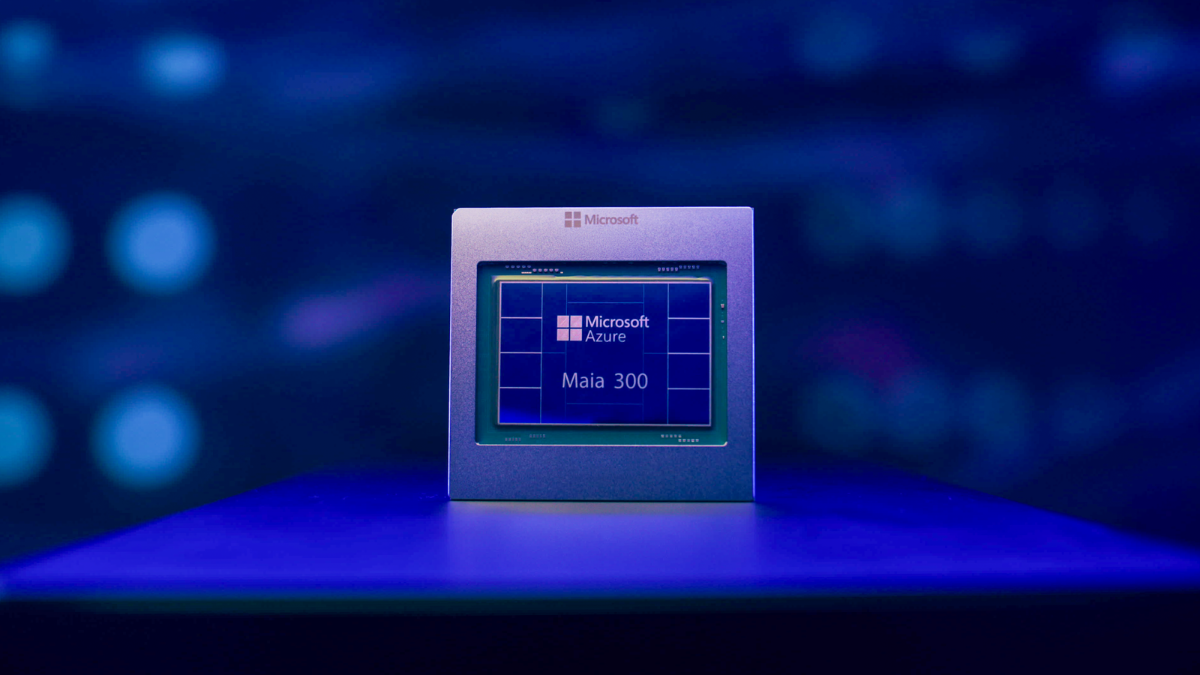
However, the highlight was the introduction of the Maia 300 AI chip, which is claimed to provide 40 percent more tokens per megawatt in comparison to other GPU-based inference systems. Further, the Maia 300 chip will serve as Microsoft’s primary AI inference platform, powering its in-house AI products and services. The AI chip has been optimised for long-context, memory-intensive, and decode-heavy AI workloads. It can balance compute, memory bandwidth, networking, and power efficiency at cloud scale.
The new Maia 300 AI chip is capable of moving data efficiently, owing to its software-defined dataflow architecture, working with AI-assisted kernel optimisation. It is also claimed to provide higher HBM bandwidth per watt, with the help of eight HBM4 stacks, offering 18TB/s of peak memory bandwidth within a 950W TDP. It is built on TSMC’s N2P process node. The AI chip has an HBM capacity of 288GB, a two-tier Ethernet scale-up with AI Transport, and 96 Maia per rack pod size.
Get your daily dose of tech news, reviews, and insights, in under 80 characters on Gadgets 360 Turbo. Connect with fellow tech lovers on our Forum. Follow us on X, Facebook, WhatsApp, Threads and Google News for instant updates. Catch all the action on our YouTube channel.